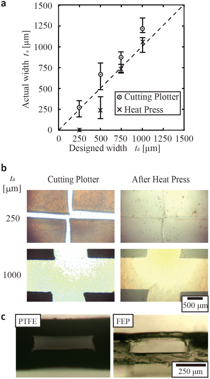
FIG. 3.
(a) A plot showing the relationship between the designed width (td) and the actual width (ta) of the straight segment of the PTFE channel (film thickness = 200 μm). (b) Representative optical micrographs showing the changes in the dimension of the channels by heat press. The opening in a stencil was fully collapsed after the heat press for the channels with td = 250 μm, while the change was not as prominent for the channels with td = 1000 μm. (c) Optical micrographs showing the cross sections of the channels formed using this method of fabrication for PTFE (film thickness = 200 μm) and FEP films (film thickness = 150 μm). Each device was created by sealing three layers of the same films by heat press.

