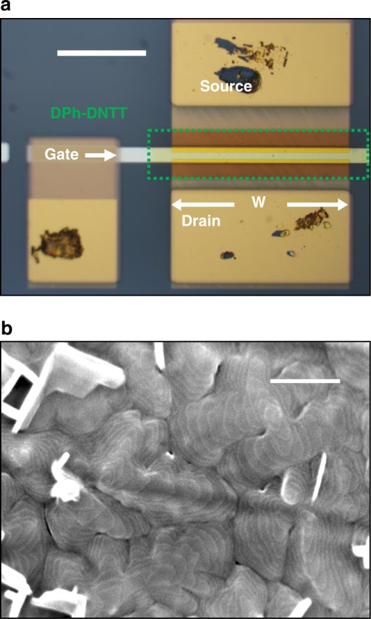
Fig. 4.

DPh-DNTT TFTs fabricated on flexible PEN substrates. a Optical microscopy image of a bottom-contact TFT with a channel length of 8 µm, a total gate-to-contact overlap (sum of the gate-to-source and gate-to-drain overlaps) of 10 µm, and a channel width of 200 µm on a flexible PEN substrate. The scale bar corresponds to 100 µm. b SEM image of the DPh-DNTT film in the channel region of a bottom-contact TFT on the same substrate. The terrace-like morphology of the organic semiconductor film is clearly distinguished and similar to that formed on the silicon substrates with atomic-layer-deposited aluminum oxide. The scale bar corresponds to 200 nm
