Fig. 1.
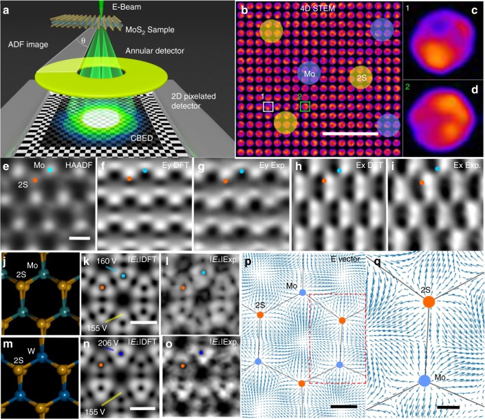
Atomic resolution 4D STEM of pristine MoS2 and WS2. a Schematic illustration of the 4D STEM geometry used. b 4D STEM data plotted as montage of CBED patterns, showing variations as a function of probe position relative to Mo and 2S atom positions. Scale bar indicates 0.2 nm. c CBED pattern from the position marked with the white box 1 in b, and d CBED pattern from the position marked with the green box in b. e HAADF-STEM image of MoS2 taken using the ADF detector. Scale bar indicates 0.2 nm. f DFT-calculated E┴y field around MoS2. g Experimental E┴y field around MoS2 measured from Icomy, normalized and scaled to the range matching the DFT values. h DFT-calculated E┴x field around MoS2. i Experimental E┴x field around MoS2 measured from Icomx, scaled to the range matching the DFT values. j Atomic model of MoS2 in a tilted projection to show 2S column. k DFT calculated |E┴| around MoS2, according to the atomic model in (j). Scale bar indicates 0.2 nm. l Experimental |E┴| around MoS2 measured from the Icom, scaled to the range matching the DFT data. m Atomic model of WS2 in a tilted projection to show 2S column. n DFT calculated |E┴| around WS2, according to the atomic model in m. Scale bar indicates 0.2 nm. o Experimental |E┴| around WS2 measured from Icom, scaled to the range matching the DFT data. Orange dots in e−n indicate S atoms position, cyan dots represent Mo and blue dots W. p 2D map of the E┴ vector, from the Icom vector, in arrow representation (arrow size indicates the magnitude of vector) around the MoS2 lattice. Scale bar indicates 0.1 nm. q Magnified view from the red dashed boxed area in p showing a high-resolution E┴ vector plot around a single Mo atom and 2S column. Scale bar indicates 0.05 nm

