Fig. 3.
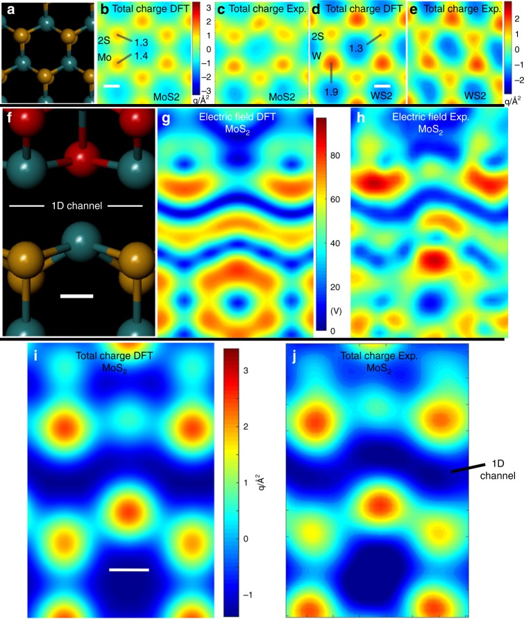
High-resolution analysis of electric field and total charge around pristine WS2 and a 1D line vacancy in MoS2. a Atomic model of MoS2, (b) total charge map from DFT calculations for MoS2 (scale bar indicates 0.1 nm and is applicable to panels (a–e)). Units are in elementary charge per Angstrom2 and c experimental total charge map for MoS2. d Total charge map from DFT calculations for WS2 (scale bar indicates 0.1 nm and is applicable to panels (d) and e and e total experimental charge map of WS2. f Atomic model of the 1D channel Mo−Mo bonding region in MoS2 line defects (scale bar in panel (f) indicates 0.1 nm and is applicable to panels (f)−(h)). g |E┴| map calculated using DFT and h experimental |E┴| map for MoS2. i Total charge map calculated from DFT for MoS2 from the atomic model in panel (f) (scale bar indicates 0.1 nm and is applicable to panels (i) and j and j corresponding total experimental charge map

