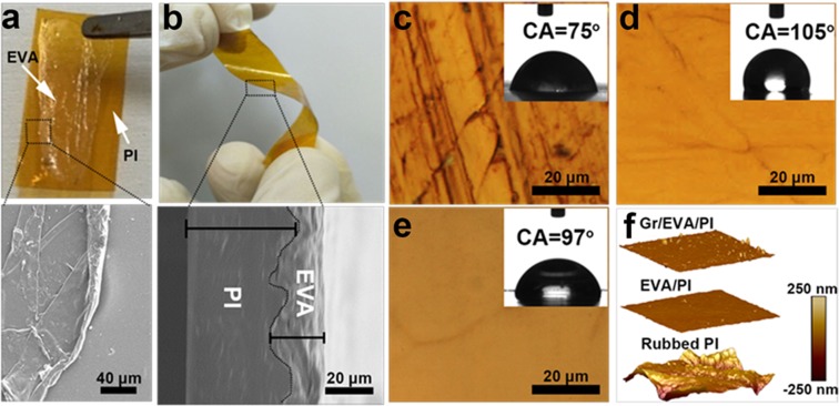
Figure 2.
Surface engineering of FTPs: Photograph of PI/EVA/graphene before surface engineering (a) and after surface engineering (b); dotted square in (a) shows that the EVA/graphene adhesivity on PI is very weak, where dotted square (b) is spotted for vertical cross-sectional SEM image revealing tight adhesion of EVA with FTPs. (c) OM image of PI rubbed with sand paper, EVA coated on rubbed PI (d) and EVA/graphene transferred onto the EVA coated PI (e), where inset shows the contact angle measurement of the respective samples. (f) AFM image to show the surface morphology of rubbed PI (bottom), EVA coated PI (middle), and graphene transferred onto the EVA coated PI (top).

