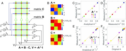
Fig. 2.
Inversion of a mixed matrix. (A) Schematic of two cross-point-array circuit for matrix inversion, where two cross-point arrays contain the elements of matrices B (Bottom) and C (Top) with A = B − C. The voltage in matrix C is inverted in the other by analog inverters, while the input current is injected in virtual-ground lines and split in the two matrices. (B) Measured values of the matrices A, B, and C, with A = B − C. In the experiment, matrix B was implemented by a cross-point array of RRAM, while matrix C was implemented by a cross-point array of discrete resistors. (C) Measured values of the inverse matrix A−1 as a function of the analytically calculated elements of A−1. As A−1 is a positive matrix, it can be inverted by a single cross-point array as in Fig. 1. (D) Conductance values for matrix A−1 implemented in RRAM elements, as a function of the experimental values of A−1 in C. To make the devices work in the high-conductance region, the matrix A-1 was implemented with G0 = 500 μS for RRAM conductance. (E) Measured elements of matrix (A−1)−1 as a function of analytical calculations. I0 = 500 μA and V0 = 1 V were used for input current and output voltage, respectively. (F) Measured elements of matrix (A−1)−1 as a function with the original matrix A, showing a remarkable accuracy despite the accumulated errors over the two sequential inversion processes and the device-programming process.

