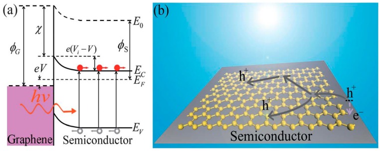
Figure 25.
(a) Energy diagram of a semiconductor/G Schottky junction solar cell under illumination. ØG and ØS are the work functions of graphene and the semiconductor, respectively. eVi is the built-in potential, V is the output voltage, EC, EV, and EF correspond to the conduction band edge, valence band edge, and Fermi level of semiconductor, respectively, and E0 is the vacuum level. (b) Schematic illustration of G-based Schottky junction solar cell. Photogenerated holes (h+) and electrons (e−) are driven towards the G and semiconductor layers, respectively. Taken from [146].

