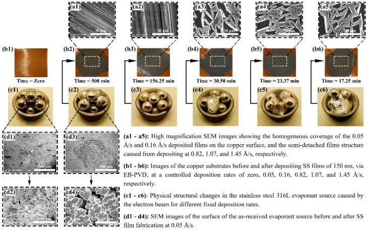
Figure 3.
Characterisation of the Stainless steel evaporant source and deposited thin films, where (a1–a5) shows the SEM images of the 0.05–1.45 Å/s as-deposited films structure, (b1–b6) illustrates the copper substrates before and after SS deposition, (c1–c6) demonstrates the physical changes in evaporant source caused by different deposition rates, and (d1–d4) shows the SEM images of the evaporant source before and after 0.05 Å/s film deposition.

