Figure 2.
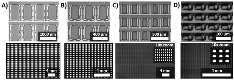
The SD chip design digitizes samples over a range of well volumes and numbers. Top row: photographs of device masters; bottom row: fluorescence images of digitized samples containing fluorescein (A shows full array, B-D are partial arrays to facilitate visualization). Four SD chips were designed with different well numbers and dimensions: (A) 640 wells (1000 μm long × 520 μm wide × 200 μm tall per well) with individual well volumes of ~100 nL and a total volume of >60 μL; (B) 1024 wells (400 μm (l) × 200 μm (w) × 100 μm (h) per well) with individual well volumes of ~7.5 nL and a total volume of ~8 μL; (C) 25,600 wells (160 μm (l) × 80 μm (w) × 80 μm (h) per well) with a well volume of ~1 nL and a total volume of >25 μL; D) 10,240 wells (30 μm (l) × 50 μm (w) × 35 μm (h) per well) with a well volume of ~50 pL and a total volume of ~0.5 μL..

