Fig. 1.
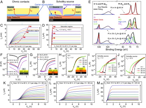
Designing and optimizing SGTs through tuning source contact deposition conditions and semiconductor thickness. (A) Structure and conduction path in a TFT with ohmic contacts. (B) Structure and conduction path in a TFT with Schottky contacts showing how the current saturates due to depletion under the source. (C and D) Typical output curves for a TFT (C) and an SGT (D); the significant difference in saturation voltage occurs because the SGT is so easily depleted beneath the source. (E) XPS results for Pt films sputtered at 60 W in Ar (Top), 60 W in /Ar (Middle), and 40 W in /Ar (Bottom). (F) curves for Pt–IGZO Schottky diodes with different powers and oxygen contents during Pt deposition (device structure in Inset). (G) Transfer curves for Pt–IGZO SGTs with different powers and oxygen contents during Pt deposition (device structure in Inset). (H–J) Transfer characteristics displaying the thickness dependence of IGZO TFTs (H) at V (device structure in Inset), SGTs at V (I), and SGTs at V (J). (K–M) Output characteristics for SGTs with 50-nm (K), 30-nm (L), and 20-nm (M) IGZO thickness. Fabricated TFTs and SGTs have source lengths mm and channel lengths m.

