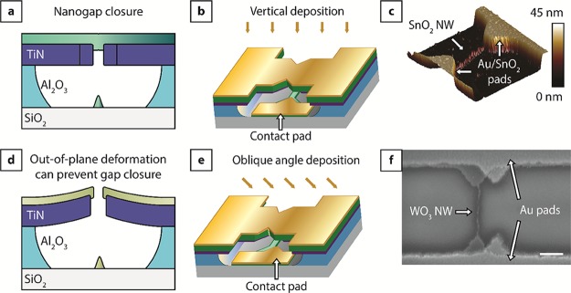
Figure 3.
Fabrication schemes for contact metallization of single NWs. (a) Schematic drawing of nanogap closure. (b) Schematics for self-aligned contact metallization for closed nanogaps. (c) AFM image of a single NW with metal contacts, where we first deposited SnO2 until nanogap closure and then deposited Au to create self-aligned electrical probing pads connecting the NW. Scale bar, 200 nm. The AFM image provides a clearer view of the SnO2 NW. (d) Schematic drawing of a nonclosed nanogap due to out-of-plane deformation of the shadow mask during deposition. (e) Schematic drawing for self-aligned contact metallization for nonclosed nanogaps. (f) SEM top-view image of a single NW, where WO3 was deposited without achieving nanogap closure. The subsequent oblique angle evaporation of Au then achieved contact metallization without forming a second NW, which would have otherwise covered the WO3 NW. Scale bar, 200 nm.

