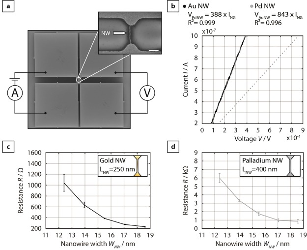
Figure 4.
Electrical characterization of single NW devices. (a) Four-point configuration for electrical characterization, with top-view SEM images of a complete device and inset with a single NW. Scale bars: 20 μm for the complete device and 200 nm for the inset. (b) I–V curves of single NW devices made of Au and Pd featuring the same geometry, exhibiting linear I–V relations. The width and length of the NWs were 20 and 400 nm, respectively. The values of resistance of the NWs are approximately 1 order of magnitude higher than the ones calculated using the bulk sheet resistance for Au and Pd, indicating that the electrical conduction is influenced by the surface roughness scattering in the polycrystalline NW structures. (c,d) Graph showing the electrical resistance of single NW devices made of Au and Pd vs WNW, respectively.

