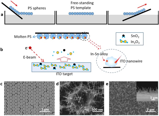
Figure 1.
Fabrication process of ITO nanowire networks. (a) Self-assembly process of PS spheres on substrate. The master was treated 30 s with oxygen plasma to get a hydrophilic surface. The PS sphere dispersion slowly reached the surface of deionized water along the master. The spheres were gathered into a monolayer film by using sodium dodecyl sulfate (SDS). The substrate was inserted below the PS sphere membrane, and then was made outward by a small angle and a slow rate. (b) ITO source (In2O3:SnO2 = 90:10, wt%) was deposited on the template by e-beam at a deposition rate of 0.1 nm/s for 20 min, with the chamber temperature stabilizing at 300 °C and pressure less than 5 × 10⁻⁴ Pa. It took 5 min to hold the surface of PS spheres in molten state before depositing. In-Sn alloy were absorbed by the melted PS spheres, and the nanowires grew based on these nucleation point. (c) The PS assembly on substrate. (d) ITO nanowires were growing based on melted PS sphere. (e) The ITO nanowire network was fabricated by annealing at 470 °C for 5 min.

