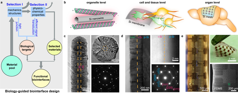
Figure 1 |. Si structures for multiscale biointerfaces.

a, A schematic diagram illustrating the principle of biology-guided biointerface design. The intended biological targets place selection criteria for material structure (I) and function (II), so that the selected materials would display a better chance to establish functional biointerfaces. b, Silicon-based materials, e.g., nanowires (left), thin membranes (middle), and distributed meshes (right), are chosen after Selection I to form tight interfaces with various biological targets, spanning multiple length scales, e.g., organelles (left), single cells or small tissues (middle), and organs (right). c, An intrinsic-intrinsic coaxial Si nanowire is synthesized from the deposition of a thick shell over a thin VLS-grown nanowire backbone as shown in a side-view TEM image (left). A cross-sectional TEM image (upper right) shows diameters of ~ 50 nm and ~ 270 nm for the core and shell, respectively. A corresponding SAED pattern (lower right) confirms the nanocrystalline structure. Orange dashed lines highlight the core/shell boundaries. d, A multilayered p-i-n Si diode junction made by a CVD synthesis of intrinsic (magenta) and n-type (green) Si layers onto a p-type (cyan) Si SOI substrate. A cross-sectional TEM image (left) shows the columnar structures of the intrinsic and n-type layers. A low-angle annular dark field scanning TEM (LAADF STEM) image (upper right) and a SAED (zone axis B = [011], lower right) pattern taken at the p-type (cyan)/intrinsic (magenta) interface both highlight the single crystalline p-type layer (isolated spots (blue) from SAED, periodic atomic columns from STEM) and the nanocrystalline intrinsic layer (concentric rings (magenta) from SAED, small crystal domains from STEM). A sharp and oxide free interface is evident from the STEM image with a junction width of < 1 nm. Orange dashed lines mark the intrinsic/n-type (left) and the p-type/intrinsic (upper right) interfaces. e, A flexible device composed of a stack of a distributed Si mesh and a holey PDMS membrane. The flexibility is demonstrated by optical (left) and scanning electron (lower right) micrographs and a photograph (upper right) taken from the same device under rolling or bending.
