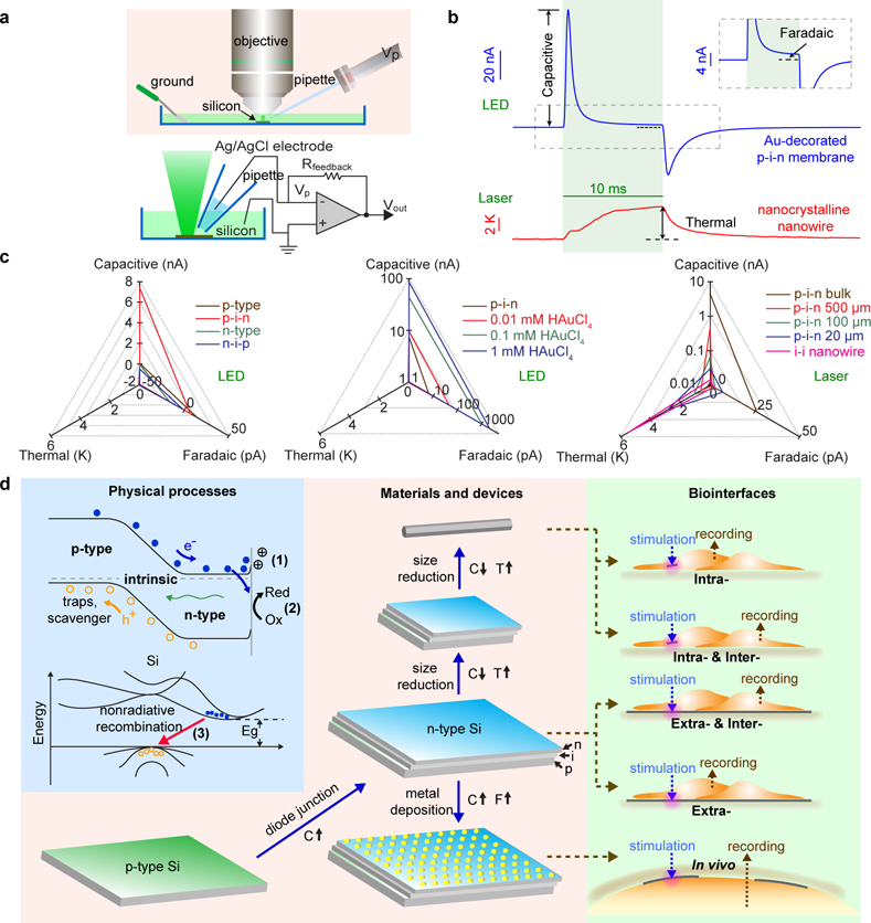
Figure 2 |. Photo-responses of Si materials.

a, Schematic diagrams illustrating the experimental setup for the photo-response measurements from Si structures. Light pulses (530 nm LED or 532 nm laser) are delivered through a water-immersion objective to the Si submerged in a PBS solution. Light-induced currents are recorded at different pipette command potentials (Vp) using a voltage-clamp mode, from which capacitive, Faradaic and thermal components can be either directly measured or derived by mathematic fitting. b, Representative photo-responses of an Au-decorated p-i-n Si diode junction (top, from 1 mM HAuCl4, LED illumination, ~ 12.05 mW, ~ 500 μm spot size, ~ 6 W/cm2) and an i-i nanocrystalline nanowire (bottom, laser illumination, 47.1 mW, ~ 5 μm spot size, ~ 240 kW/cm2) showing three major types of the responses, i.e., capacitive (upper), Faradaic (upper inset), and thermal (lower). LED-induced capacitive and Faradaic currents are pronounced in the Au-decorated diode junction. The capacitive current is defined as the maximal current amplitude reached after the light onset while the Faradaic current is defined as the current amplitude at the time point of 8.5 ms since illumination starts. The nanocrystalline nanowire generate significant heating of the surrounding PBS via its photothermal effect under laser illumination. Green shaded areas highlight the light illumination periods. The grey dashed box marks the region for the inset. c, Quantitative matrices of the three photo-responses, used to evaluate the impact of important materials parameters, e.g., doping (left), surface chemistry (middle), and size (right). Diode junctions (left, p-i-n and n-i-p) show significantly enhanced capacitive currents versus uniformly doped SOI substrates (p-type and n-type). Au-decorated p-i-n diode junctions (middle) promote both capacitive and Faradaic currents. Si structures with smaller dimensions (right) show stronger photothermal responses. d, A principle for Selection II (Fig. 1a), highlighting the physical origins (light blue block), the material developing pathways (light orange block), and the projected biointerfaces (light green block). Fundamental processes include the accumulation of ions to balance light-generated excessive carriers near Si surface (1, capacitive, C), the metal-mediated redox reactions (2, Faradaic, F), and the thermalization through phonon emission (3, thermal, T). Considering the size and mechanics match at the biointerfaces (i.e., Selection I, Fig. 1a), these Si structures can be utilized to form optically-controlled intra- (Si nanowires), inter- (Si nanowires and p-i-n diode junctions), and extra-cellular (pristine and metal-decorated p-i-n diode junctions) biointerfaces.
