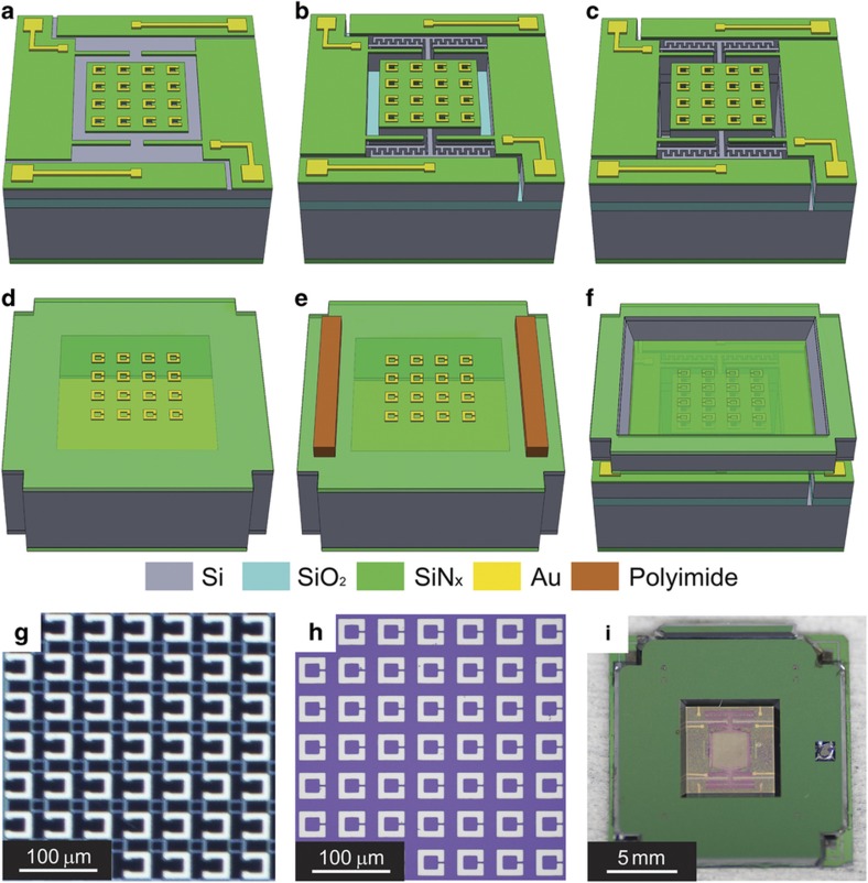
Figure 2.
(a–c) Process flow to fabricate Chip 1 on SOI wafer. (d–e) Process flow to fabricate chip 2 on silicon wafer. (f) Flip-chip bonding to align and bond the two chips. (g and h) Microscopic images of the SRRs on Chip 1 and Chip 2, respectively. The capacitive gaps are 16 μm in Chip 1 and 2 μm in Chip 2. (i) Picture of the bonded device.

