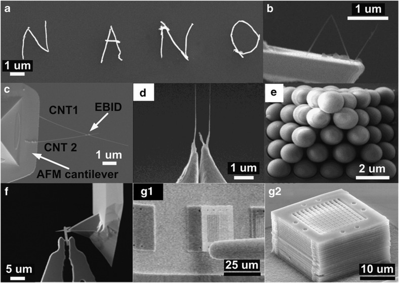
Figure 5.
Examples of nano device and nanostructure assembly. (a) Nanowires were picked and placed to assemble a nano pattern. Adapted from Ref. 163. (b) A MWCNT was formed using a 3D letter with EBID. Adapted from Ref. 13. (c and d) A thermal sensor and a pair of nanoscaled tweezers were assembled with nanomanipulation. Reprinted with Institute of Physics Publishing (IOP) permission from Ref. 138 and adapted from Ref. 165. (e) 3D pyramidal spheres were assembled. Adapted from Ref. 70. (f) A nanotool was mounted on an AFM cantilever. Reprinted with IOP permission from Ref. 39. (g1 and g2) Assembly of photonic plates to form a 3D photonic crystal. Adapted from Ref. 1. EBID, electron-beam-induced deposition; MWCNT, multi-walled CNT.

