Figure 1.
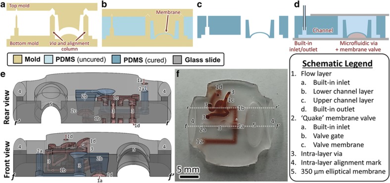
Illustration of fabrication process (top) and technical capabilities (bottom) of 3D-printed transfer molding for double-sided microfluidic devices. Fabrication: (a) mold is 3D-printed from a CAD model, treated, fitted using alignment marks, and (b) filled with PDMS and cured. Excess PDMS is cut away and the mold is removed. (c) The resulting PDMS component contains integrated inlets/outlets, membranes, and vias, and is (d) bonded to glass to create a device with enclosed channels of arbitrary cross-section. Technical capabilities: the multilevel microfluidic device shown in cross-section in (e) and photographed in (f) is fabricated using double-sided molding techniques and exhibits numerous design elements, such as two-layer fluid flow, multiple microfluidic vias, integrated fluid inlets/outlets, an elliptical 350-μm domed membrane, and a “Quake”-style membrane value, as well as alignment marks for use in generating multilayer devices. 3D, three-dimensional; PDMS, poly(dimethylsiloxane).

