Figure 3.
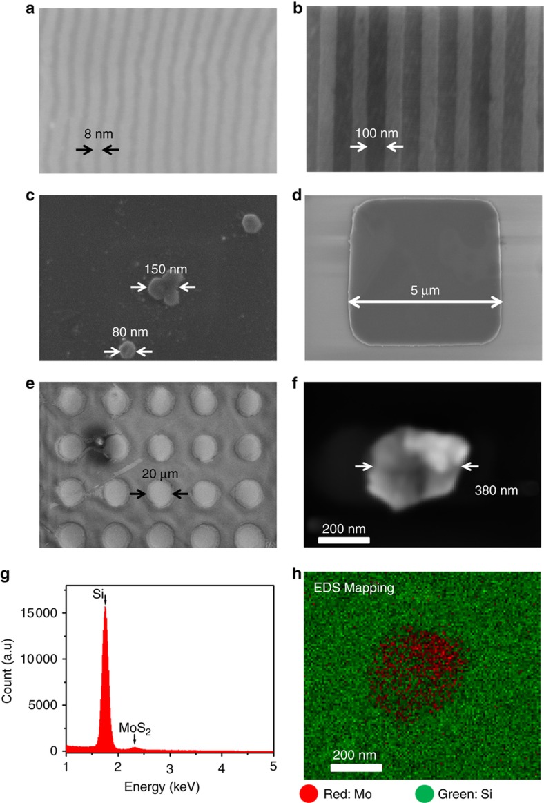
SEM images of representative good-quality MoS2 nano- and microstructures produced via NASE+TP processes, including (a) 8 nm half-pitch, 1.3 nm-thick line-spacing patterns, (b) 100 nm half-pitch, 3.3 nm-thick line-spacing patterns, (c) 80–150 nm size, 10 nm-thick mesas, (d) 5 μm size, 25 nm-thick flakes, (e) 20 μm size, 40 nm-thick flakes, and (f) a 380 nm size, 20 nm-thick flake. (g) The EDS spectrum acquired from the MoS2 nanostructure shown in (f). (h) The EDS elemental mapping of Mo and Si.

