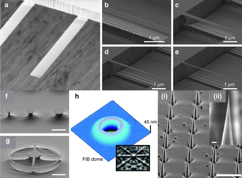
Figure 1.
(a) Scanning-electron-microscope (SEM) micrographs of 100(25) nm thin and 12 μm wide optical-grade single crystal diamond cantilevers. Image reprinted by permission from Macmillan Publishers Ltd: [Nature Communications]: Ref. 27, copyright 2014. SEM of diamond doubly clumped nanobeams with width (b) 500 nm, (c) 350 nm, (d) 200 nm and (e) 75 nm. (f) ~3–5 μm diameter undercut micro-disks; and (g) ~500 nm wide nano ring structure. Images reprinted (adapted) with permission from: Ref. 26. Copyright 2012 American Chemical Society. (h) Atomic force microscopy (AFM) image of a focused-ion-beam (FIB)-defined dome, scan size 5·5 μm2. Inset shows an electron backscatter diffraction (EBSD) pattern confirming the single-crystal nature of the device layer. Image reprinted with permission from: Ref. 36. Copyright 2011 American Chemical Society). (i) Regular array of lithographically defined single crystal diamond tips (scale bar, 10 μm) and (ii) zoom in after cleavage resulting in sharp tips with radii of about 10 nm. The scale bar is 100 nm. Images reprinted (adapted) with permission from: Ref. 37. Copyright 2015 American Chemical Society.

