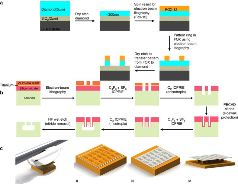
Figure 6.
Examples of diamond nanofabrication and patterning. (a) Dry etching (oxygen plasma in an Oxford RIE etching machine) thin-down technique of 5 μm-thick diamond membrane until it is 300 nm thick placed on a 2 μm-thick SiO2 layer grown on a silicon wafer. The electron-beam resist (Fox12) is spun on the chip and electron-beam lithography used to pattern a ring resonator. The pattern is transferred from the resist to the diamond using dry etching in an oxygen plasma. Image available under the terms of the Creative Commons Attribution 3.0 License from Ref. 57. (b) Process for fabrication of diamond nanobeams using quasi-isotropic reactive-ion undercut etching. Image available under the terms of the Creative Commons Attribution 3.0 License from Ref. 32. (c) Patterning of a diamond membrane using a silicon membrane as a contact etch mask. (I) Transferring of a Si mask onto a <300 nm diamond membrane using a micro PDMS adhesive. (II) The silicon membrane on top of the diamond membrane is used as an etch mask for oxygen plasma etching. (III) The diamond membrane is patterned during oxygen etching with subsequent mask removal. (IV) A SF6 isotropic dry etching removed the silicon underneath and suspended the diamond membrane. Image reprinted by permission from Macmillan Publishers Ltd: [Scientific Reports]: Ref. 69, copyright 2015.

