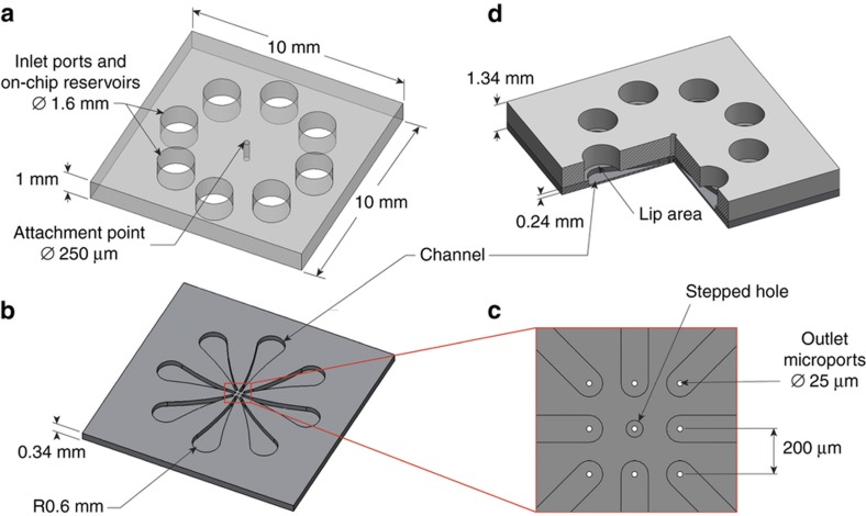
Figure 2.
Component design and assembly detail of the prototype artificial chemical synapse chip. (a) A solid-model of the top glass layer, 10 mm×10 mm×1 mm in size, featuring eight 1.6 mm-diameter through holes, equally spaced around a circle of 6.4 mm diameter, that serve as on-chip reservoirs and a 250 μm-diameter through hole at the center that serves as an attachment point where the device is anchored to a manipulator arm during experiments. (b) A solid-model of the bottom silicon layer, 10 mm×10 mm×340 μm in size, featuring eight 240 μm-deep tapered microchannels with the narrow end of each microchannel feeding into a microport near the center of the chip. (c) A close-up view of the eight 25 μm-diameter through holes that serve as microports for glutamate delivery and a 25 μm-diameter stepped hole (25 μm-diameter through hole followed by a 75 μm-diameter and 240 μm-deep hole) at the center that serves as an alignment feature during the device assembly. The eight microports are laid along the periphery of a 3×3 array with a spacing of 200 μm between any two adjacent microports and the larger alignment hole at the center of the chip is not connected to any reservoir and thus not utilized for glutamate injections. (d) A quarter cutout-view of the assembled device after integrating the top glass layer and the bottom silicon layer. The hatched region shows the interior details of a reservoir hole aligned with the larger end of a tapered channel with a small lip area at the bottom of the reservoir hole and the smaller end of the tapered channel feeding into a microport. The purpose of the lip area at the bottom of the reservoir is to firmly seat one end of a flexible tube supplying pressure pulses inside the reservoir hole without blocking the channel. This design allows each microport to be addressed independently by actuating the connected reservoir port selectively.

