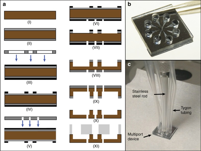
Figure 3.
Fabrication and assembly of the prototype artificial chemical synapse chip components. (a) Cross-section diagrams illustrating select steps of the process flow for microfabrication of silicon layer. I. Clean silicon wafer, 340 μm thick, II. Deposition of 450 nm-thick aluminum mask layer for the DRIE process, III. Photolithography of microchannels and the larger (75 μm diameter) end of the stepped hole on the top side of the silicon wafer, IV. Development of the exposed regions on the top side with AZ developer, V. Photolithography of microports and the smaller (25 μm diameter) end of the stepped hole on bottom side of the silicon wafer, VI. Development of the exposed regions on the bottom side with AZ developer, VII. Exposed aluminum layer etched with PAN etch, VIII. Tapered microchannels and the larger end of the stepped hole etched to a depth of 240 μm on the top side of the silicon wafer using DRIE, IX. Eight microports and the smaller end of the stepped hole etched to a depth of 100 μm from the bottom side of the silicon wafer using DRIE, X. Aluminum mask layer stripped and the wafer diced into dies, XI. Glass layer chip, fabricated separately, aligned and bonded to the silicon chip using anodic bonding. (b) A photograph of the completely fabricated prototype of the device held by tweezers. (c) A photograph showing Tygon tubing and manipulation rod attached to the prototype device. Each Tygon tube connects each reservoir in the device to an independent channel of a multichannel pressure injector for actuation and the manipulation rod is used to anchor the device to a manipulator for maneuvering the device during experiments.

