Figure 4.
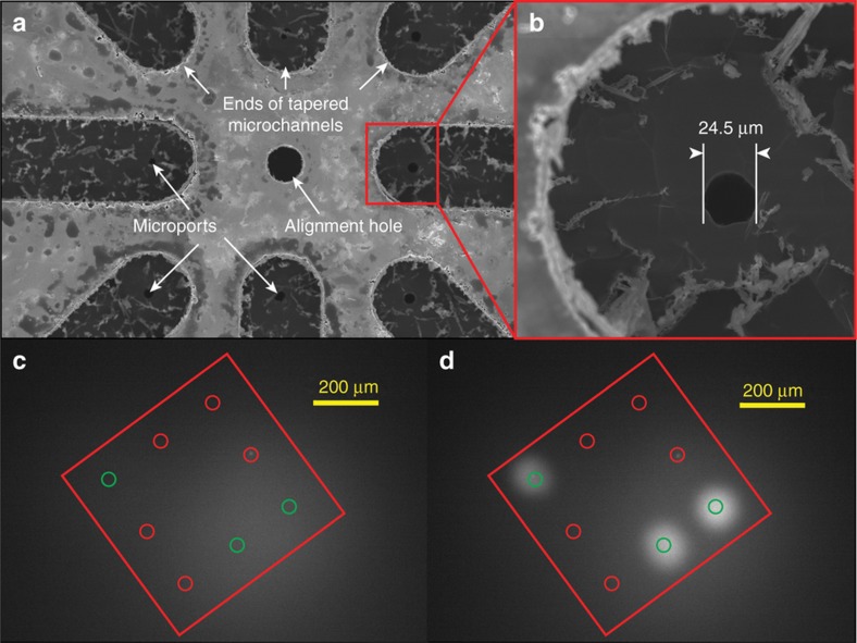
Experimental characterization of the prototype artificial chemical synapse chip device. (a) A scanning electron microscope (SEM) image of the eight microports near the center of the silicon layer chip after the DRIE process. The images confirm the openings of all microports and smaller ends of the tapered microchannels feeding into the microports per design. (b) An SEM image showing a close up view of a microport hole near the smaller end of the tapered microchannel. The diameters of the holes measured under the microscope from the channel side varied from the intended diameter (25 μm) by about 0.5 μm across all holes yielding an average diameter of 24.5 μm. The variation in hole diameters is attributable to the effects of DRIE etch rate variations within the die including microloading and local pattern density around the microports. (c and d) Epifluorescent images characterizing the device before and after injecting fluorescein water solution into clear water, respectively. To verify the function and independent actuation of each microchannel and associated microport, water mixed with 0.01% fluorescein dye was injected into a Petri dish containing clear water through all microports, one-by-one, as well as a select subset of microports simultaneously by pneumatically actuating the respective reservoir(s). Active microports (green circles) were identified and distinguished from the inactive microports (red circles) by observing a discernable increase in fluorescence around the active microport(s) immediately after the injections, such as the three microports shown in (d), compared to the inactive microports and the initial state of the microports before the injections as in the control image shown in (c). This fluorescence microscopy-based characterization of flow through various microports of the device verified that no two channels were inadvertently cross-connected via micro gaps at the interface of the layers due to poor bonding and all active microports could be addressed independently.

