Figure 1.
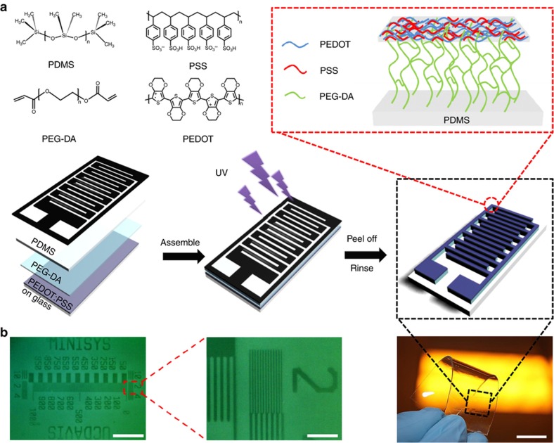
(a) Schematic illustration of the one-step photopatterning method to produce the PEDOT:PSS/PEG hybrid thin film, molecular structures of PEDOT:PSS, PEGDA, and PDMS, interactions between each layer, and an optical image of patterning the hybrid film on a PDMS substrate (scale bar, 1 cm). (b) Optical microscopy image of the patterned PEDOT:PSS/PEG hybrid film on PDMS (scale bar, 500 μm) and a magnified image showing feature resolution as small as 2 μm (scale bar, 50 μm).

