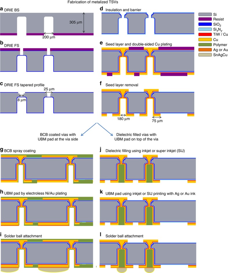
Figure 2.
(a–f) Process flow for the TSV fabrication9. (g–i) Conventional fabrication approach with solder balls placed next to the via holes, resulting in low I/O densities, as in Ref. 10. (j–l) Approach demonstrated in this work with TSVs filled with inkjet-printed dielectric polymer and solder balls placed in the same area as the TSVs to increase the I/O density. I/O, input/output; TSV, through silicon via.

