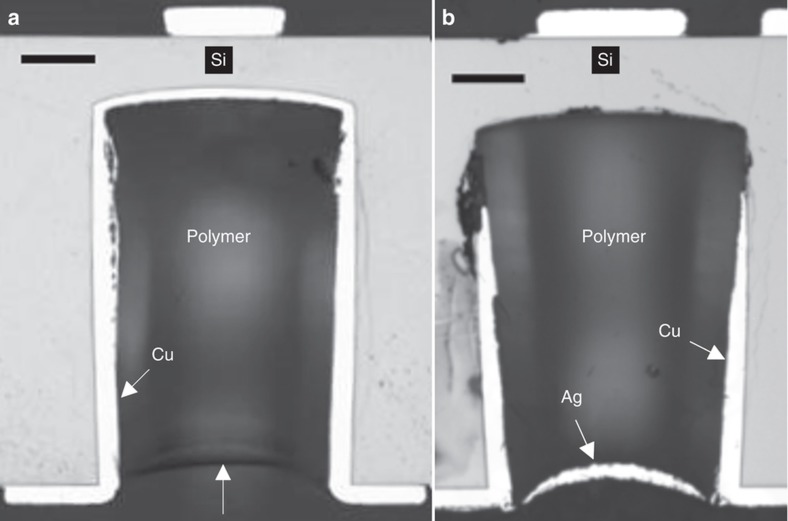
Figure 4.
(a) Cross-sectional image of the TSV after successful dielectric filling by inkjet printing, where the white arrow at the bottom shows the surface of the dielectric layer. (b) Cross-sectional image of the TSV with the Ag UBM layer on top of the dielectric material. Scale bars are 50 μm. TSV, through silicon via; UBM, under bump metallization.

