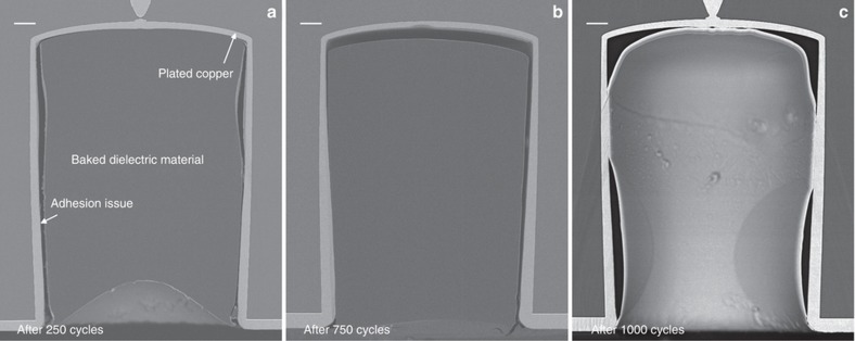
Figure 7.
BIB prepared cross-section SEM images of the filled vias after temperature cycling tests with (a) 250 cycles, (b) 750 cycles, and (c) 1000 cycles. Scale bars are 20 μm. In (b), the connection between the via metallization and the FS RDL on the top wafer surface cannot be seen because the cross section is not exactly passing through the center of the via. BIB, broad ion beam; FS RDL, frontside redistribution layer; SEM, scanning electron microscope.

