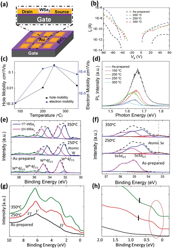
Figure 5.

Transport, photoluminescence, and photoemission measurements of WSe2/Au at various annealing temperatures. a) Device structure schematic of a WSe2 field‐effect transistor. b) I d–V g of the WSe2 device as functions of annealing temperature. c) Hole and electron mobility at different gate voltages of the device as functions of annealing temperature. d) Annealing temperature dependence of photoluminescence spectra. e,f) Synchrotron‐based X‐ray photoemission spectra of W4f, W5p3/2, and Se3d core‐level peak regions for WSe2 on Au film annealed at various temperatures. These spectra can be well fitted by two components with constant peak positions and full width at half maximum (FWHM). g) Valence band and h) narrow valence band for WSe2 on Au film annealed at various temperatures. The Fermi surface feature is indicated by the dashed red circle while the mid‐gap feature positions denoted by the black vertical markings (see the Experimental Section for details).
