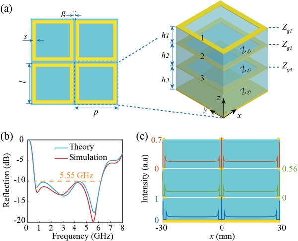
Figure 2.

The design of the broadband absorber. a) The schematic of the absorber. Based on the catenary model, the response of this structure can be calculated directly that the parameters of this structure can be optimized to realize efficient absorption. The optimized parameters are p = 30 mm, g = 0.2 mm, s 1 = s 2 = 1 mm, s 3 = 1.5 mm. h 1 = 13 mm, h 2 = h 3 = 18 mm. Rs 1 = 30 Ω, Rs 2 = Rs 3 = 22 Ω. The dielectric is set as air with ε = 1 and the metal is nichrome with conductivity σ = 2.2 × 10⁵ S m−1. Zgi, Zdi (i = 1, 2, or 3) are the effective impedance of the metasurface and the impedance of dielectric. b) Simulated and theoretical reflection from 0 to 8 GHz. The −10 dB bandwidth of our structure is 5.55 GHz with more than three octave bandwidths. c) The extracted electric field distribution along the trilayered metasurface at 5.56 GHz. As the distance between adjacent resonators is much smaller than that between two arms of a resonator, the intensity of electric field is much stronger in the former case.
