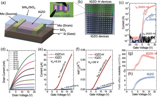
Figure 1.

Characterizations of TFTs. a) Schematic view of a TFT device. b) Optical image of TFT arrays with the upper half IGZO‐H and the lower half remains pristine, where one of the devices is shown on the left. c) Transfer characteristics (V D = 0.1 V) of IGZO‐H (red) and IGZO TFTs (blue) measured on the same substrates shown in (b). d) Output characteristics for various V GS values. e) Transfer characteristics in the linear regime (V D = 0.1 V) of IGZO‐H TFT and IGZO TFT, with the extracted linear mobility. f) Square root of drain current in the saturated regime (V D = 20 V) IGZO‐H TFT (red) and IGZO TFT (blue), with the extracted saturated mobility. Extracted field effect mobility plotted against gate voltage of IGZO‐H TFT g) and IGZO TFT h) in the linear regime (V D = 0.1 V).
