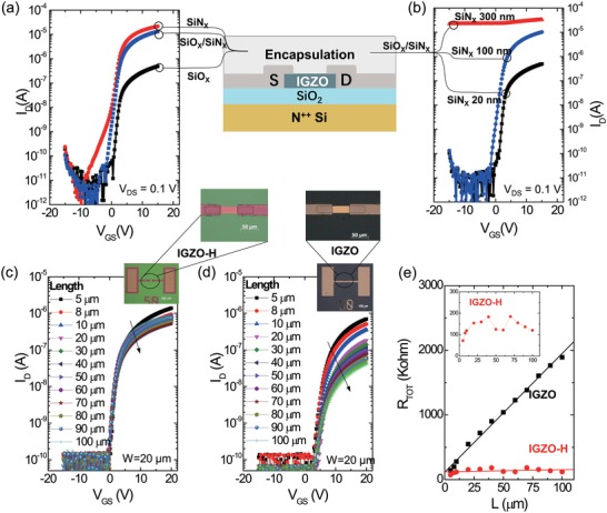
Figure 2.

Effect of encapsulation layers and channel length scaling. a) Linear transfer curves with encapsulation layer of SiOX (350 nm, black), SiNX (100 nm, red), or SiOX/SiNX (350/100 nm, blue). b) Linear transfer curves with encapsulation layer of SiOX/SiNX with varying the thickness of SiNX: 20 nm (black), 100 nm (blue), or 300 nm (red). All the devices were annealed at 350 °C for 1 h after the final deposition. Transfer characteristics (V DS = 0.1 V) of IGZO‐H c) and IGZO d) TFTs with channel length L varying from 5 to 100 µm (W = 20 µm) with optical images. The zoomed‐in images show the channel area with the semiconductor islands is narrower than the electrodes, avoiding the fringe current. e) Total resistance R TOT against L for IGZO TFTs (black) and IGZO‐H TFTs (red), with the latter enlarged as inset. The dots are measured data and the lines are linear fittings.
