
Figure 3.
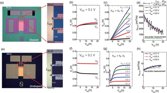
Gated four‐probe (GFP) measurements. a) Optical image of one IGZO‐H TFT and the region near the probes is enlarged on the right. b) Potential of probe A and B in IGZO‐H TFT with V DS = 0.1 V. c) Potential drop V XX = V B −V A as a function of V GS with various V DS. d) The extracted channel field‐effect mobility of IGZO‐H TFT with various V DS by GFP measurements (dots) or transfer curves of TFTs (dashed lines). The corresponding measurements of IGZO TFT are shown in (e–h).