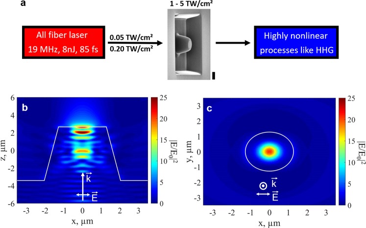
Figure 1.
Field enhancement in the semiconductor waveguide. (a) Schematics of the field enhancement. The local field enhancement increases moderate pump intensities of 0.05–0.2 TW/cm2 provided by the laser to up to 5 TW/cm2 and allows for HHG. The SEM picture shows our structure patterned on a bulk ZnO crystal with the dimensions: base size of 4.1 µm in diameter, height of 6.1 µm and top of 2.6 µm. The vertical black thick bar represents 2 µm. (b) Simulation of the intensity distribution in the cone (plane spanned by k- and E-vectors). Significant intensity enhancement occurs on the tip of the cone by a factor larger than 20. The simulation has been done with the experimental parameters. c Intensity enhancement at the exit of the cone (plane perpendicular to the propagation direction) 100 nm below the top surface of the cone.

