Figure 2.
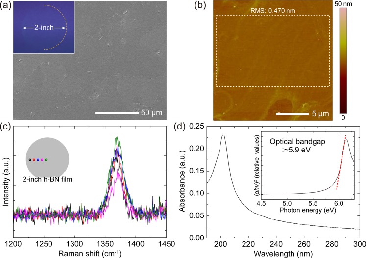
Microscopic and spectroscopic characterizations of the h-BN film grown on the Ni(111) template. (a) SEM image of as-grown h-BN film on the Ni(111). (Inset) Photograph of the 2-inch wafer-scale h-BN film transferred on a 4-inch SiO2/Si substrate. (b) AFM image of the h-BN film transferred on a SiO2/Si substrate. (c) Raman spectra of the h-BN film. (Inset) Schematic description of the representative positions where the Raman spectra were measured. (d) Absorbance spectrum of the h-BN film. (Inset) Tauc’s plot and optical band gap analysis.

