Figure 5.
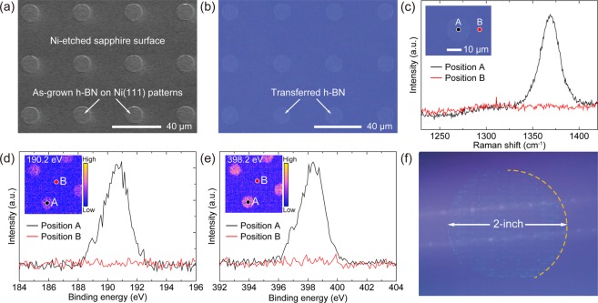
Selective-area growth of h-BN. (a) SEM image of as-grown h-BN on the pre-patterned Ni(111) template and (b) corresponding optical image after transfer onto SiO2/Si. (c) Raman spectra acquired from the positions marked in the inset optical image. Micro-focused XPS spectra of (d) B 1 s and (e) N 1 s core-levels measured at specific positions marked in the inset images. (Inset) SPEM images for selected energies of 190.2 eV and 398.2 eV over 80 × 80 μm2 scan range, respectively. (f) Photograph of the wafer-scale selective-area grown h-BN after transfer onto a 4-inch SiO2/Si substrate.

