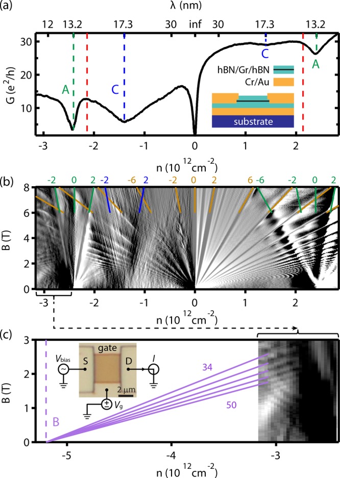
Figure 2.

Electronic transport
at 4.2 K. (a) Two-terminal differential conductance G as a function of charge carrier density n. In addition
to the MDP, there are four other conductance minima
at nsA ≈ ±2.4 ×
1012 cm–2 (green dashed lines) and nsC ≈ ±1.4 × 1012 cm–2 (blue dashed lines), respectively.
The top axis shows the moiré periods  . The red dashed lines
indicate the longest
period (lowest density) for a graphene/hBN MSL. Inset: schematic of
the cross section of our device. (b) dG/dn as a function of n and B of the same device. Filling factors fan out from all DPs, except
for the blue one on the electron side and are indicated on top of
the diagram, calculated as ν ≡ nh/(eB), where n is counted from each DP. (c)
Zoom-in on the left side of (b). There are additional lines fanning
out from an even higher density nsB ≈ 5.2 × 1012 cm–2, labeled B. The filling factors of these lines are 34, 38, 42, 46
and 50, respectively. Inset: micrograph and experimental setup of
the presented device. “S” and “D” are
the source and drain contacts, respectively.
