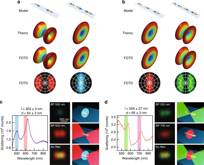
Fig. 6. Physical picture for the colour routing effects.
a, b Schematics of the theoretical models (first row), theoretically calculated 3D far-field radiation patterns (second row), FDTD-simulated 3D far-field radiation patterns (third row) and FDTD-simulated back focal plane images (fourth row) of the horizontally aligned electric dipole arrays based on the charge distribution contours shown in Fig. 4b, f, respectively. c Understanding of the colour routing effect for the red-blue-red patterns. The left side is the experimental scattering spectrum of a typical nanorod showing the red-blue-red pattern, with the two vertical bars indicating the bandpass colour filters. The middle column shows the experimental scattering images acquired with the 500-nm bandpass filter (first row), with the 600-nm bandpass filter (second row) and in the absence of a colour filter (third row) in front of the camera, together with the corresponding schematics for understanding the colour routing effect (right column). d Understanding of the colour routing effect for the green-red-green patterns. The left side is the experimental scattering spectrum of a typical nanorod showing the green-red-green pattern, with the two vertical bars indicating the bandpass colour filters. The middle column shows the scattering images acquired with the 550-nm bandpass filter (first row), with the 700-nm bandpass filter (second row) and in the absence of a colour filter (third row) in front of the camera, together with the corresponding schematics for understanding the colour routing effect (right column)

