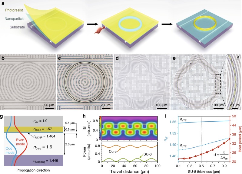
Fig. 5.
Photolithography with the UV emission for precise formation of waveguides and patterns. a Schematic design for patterning SU-8 photoresist. NaErF4@NaYF4 upconversion nanoparticles and SU-8 film are deposited on the substrate. Locally generated upconversion light by the waveguide structure induces selective exposure of SU-8 film. b, c Micrographs of a microring resonator before and after developing a SU-8 layer on the ring. d–f Micrographs of a waveguide loop before and after developing a periodic structure of SU-8. g Waveguide geometry and parameters of the simulation model with the upconversion nanoparticle (UCNP) and SU-8 upper cladding layers. h Distribution of the electric field amplitude along the propagation direction showing the beating between the odd and even modes (top) and the plot of fractional power in the core and SU-8 regions of the waveguide as a function of propagation distance (bottom). i Calculated effective indices of the even/odd modes and the beat period as a function of SU-8 thickness at 1550 nm, respectively. The period observed in (f) matches well with the calculated period Λ = λ/Δneff

