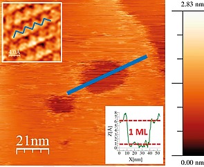
Figure 11.

STM image of craters on a bP flake, annealed at 400 °C for 5 min, measured at room temperature. The upper left inset shows an atomic resolution zoom‐in. Craters are aligned along the zigzag direction indicated by the blue lines. The lower right inset shows that the crater is monolayer‐deep. Scan parameters: 1.5 V/100 pA.
