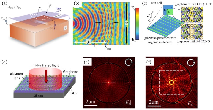
Figure 6.
In-plane plasmonic wavefront engineering. (a) Monolayer graphene on top of the uneven ground plane made of highly-doped silicon. Different distances between the graphene layer and the ground plane lead to two conductivities and two refractive indices of the SP wave in and out of the lentil area. (b) Simulated electric field of the SP wave through the graphene Fourier lens with point source excitation. Reproduce with permission from [66], Copyright Aptara Inc., 2012. (c) Schematic representation of the graphene layer patterned with two types of organic molecules (TCNQ + TTF and F4 - TCNQ) to achieve an inhomogeneous conductivity profile through charge transfer. Reproduced with permission from [43], Copyright American Chemical Society, 2014. (d) Schematic of the spiral-shaped graphene vacancy for excitation and focusing of the SP wave. (e) Superfocusing using a spiral-shaped graphene vacancy together with a circularly-polarized incident beam. (f) Generation of plasmonic vortex beam with five segmented graphene vacancies. All the in-plane wavefront shaping is achieved in a notable subwavelength area and beyond the diffraction limit considering the strong localization of the graphene plasmon. Reproduced with permission from [68], Copyright Optical Society of America, 2014.

