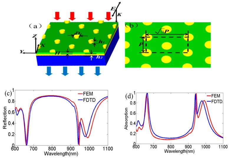
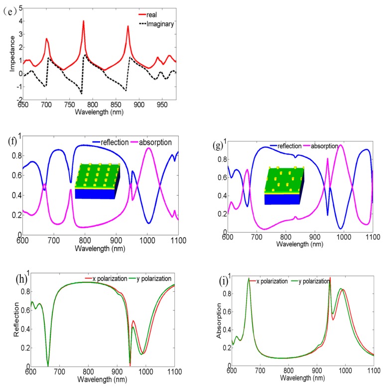
Figure 1.
Schematic view and optical properties of the hexagonal nanodisk array layered structure under normal incidence. (a) Three-dimensional view of the designed layered structure and its structural parameters; (b) top cross-section of the designed structure. Calculated spectra for (c) reflection and (d) absorption with structure parameters (P, D, h1, h2, H) = (700, 200, 50, 50, and 40 nm) by finite element method and finite-difference time domain simulation, respectively; (e) real part and imaginary part of the retrieved relative effective impedance in discussed wavelength regions. Calculated reflection (blue line) and absorption spectra (pink line) for (f) square nanodisks array and (g) honeycomb-like nanodisks array with the same structure parameters as that of discussed hexagonal nanodisks array structure. Insets of (f,g) show the schematic views of square array and honeycomb-like array, respectively. The influence of changing polarization directions onthe (h) reflection and (i) absorption spectra.


