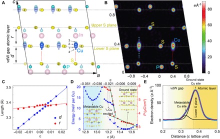
Fig. 4. Atomistic origin of the giant negative longitudinal piezoelectricity in CIPS.

(A) Refined unit cell structure of CIPS viewed along the b axis. The foremost sheet of atoms parallel to (010) plane is highlighted, while the rest are attenuated. The size of the Cu atom indicates its occupancy at the corresponding site. (B) The cross-sectional electron density map of the atomic plane highlighted in (A). The gray dashed lines denote the upper and lower sulfur planes. Red dashed lines indicate the possible interlayer Cu─S bonding across the vdW gap. (C) Calculated changes of the vdW distance d and the layer thickness r of CIPS as a function of strain along c axis. Solid lines are linear fits. (D) Evolution of the free energy E (blue) and the change of ferroelectric polarization P (red) as a function of lattice constant along the c axis under different conditions: triangle, all Cu occupying metastable site; circle, ¼ Cu occupying metastable site; square, all Cu occupying ground-state site. The insets show the corresponding atomic structures. (E) Electron density profile along the blue dashed line shown in (B). The asymmetric distribution of Cu due to the partial occupancy of the metastable site can be fitted by two Gaussian peaks (solid lines).
