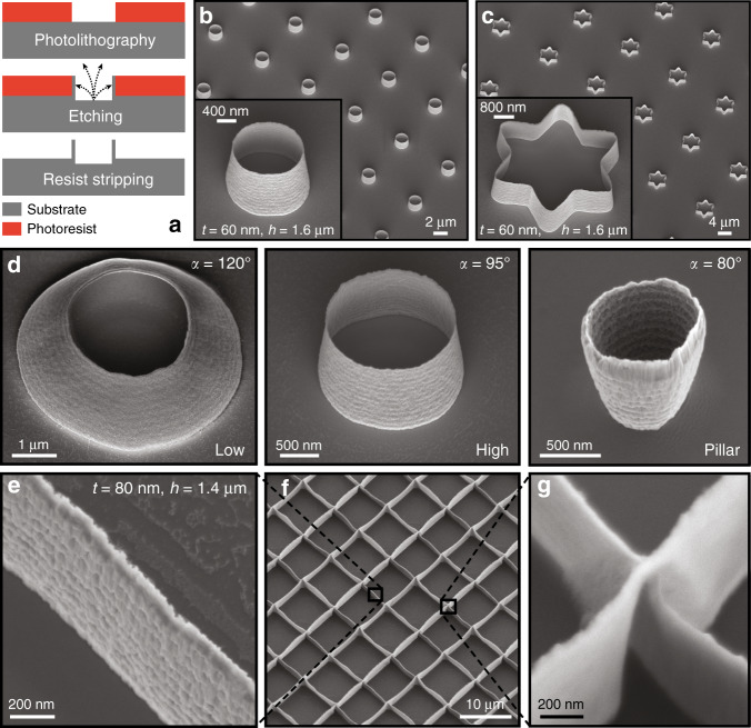
Fig. 1. Structures created by Si redeposition on photoresist sidewalls during Ar+ ion beam etching.
a Illustration of the process flow used to create Si nanostructures: during ion beam etching, the photoresist sidewalls are sputtered by the etched material and after resist stripping, nanostructures are obtained. SEM images of b cylinder arrays, c star arrays composed of 60-nm-thick and 1.6-μm-high walls, and d profiles obtained by changing the dose from low to high during photolithography. The structure profile can even become negative by performing the redeposition step on a pillar rather than a resist opening. The angle α is defined between the substrate and the cylinder wall. For a vertical wall α = 90°. e−g SEM images of 80-nm-thick and 1.4-μm-high intersecting nanowall arrays. Tilt angle of 30°. SEM scanning electron microscope

