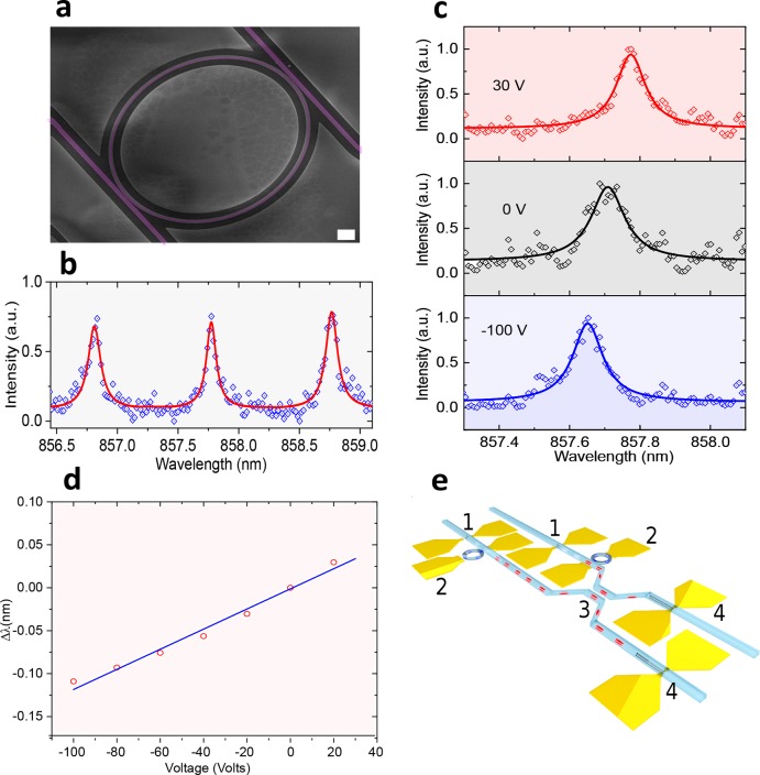
Figure 5.
(a) Scanning electron microscope image of silicon nitride ring resonator fabricated on a piezoelectric substrate, the scale bar is 2 μm. (b) Drop port transmission of the ring resonator with free spectral range of 0.96 nm. (c) Single resonance peak at different applied voltages to the PMPT–PT substrate: 30, 0, and −100 V for top, middle, and bottom panels, respectively. Negative voltages correspond to compressive biaxial strain, resulting in blue-shifting the resonance of the optical cavity. (d) Trace of the drop port transmission peak as a function of voltage. (e) Envisioned applications of strain-tunable hybrid quantum photonic circuit. The depicted circuit shows two nanowire quantum emitters (labeled “1”) strain-tuned to the same wavelength, then a filtering stage consisting of a pair of ring resonators (labeled “2”) that are strain-tuned to transmit specific optical transitions of the nanowire QD. Finally, a pair of superconducting nanowire single-photon detectors (labeled “4”) is integrated with a beam splitter (labeled “3”) to study on-chip quantum interference between remote emitters.

