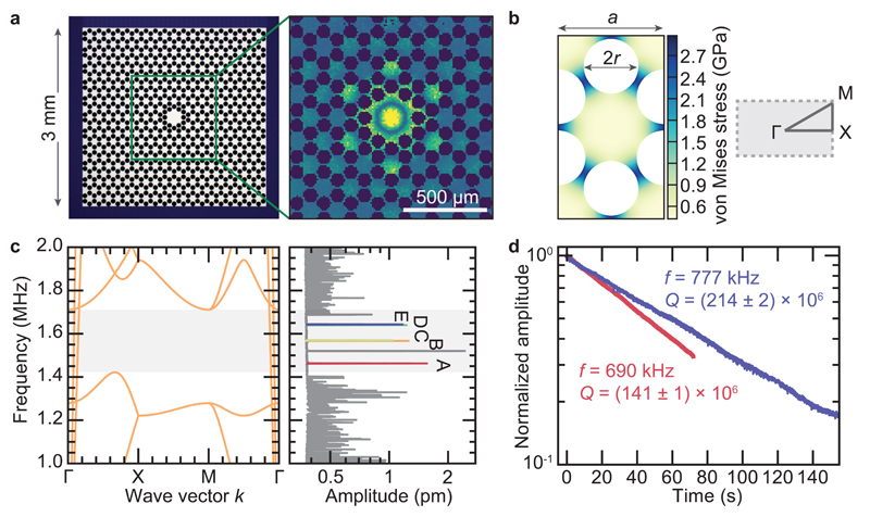
Fig. 1. Device characterisation.
a) Micrograph of a silicon nitride membrane patterned with a phononic crystal structure (left) and measured out-of-plane displacement pattern of the first localised mode “A” (right), of a device with lattice constant a = 160µm. b) Simulation of the stress redistribution in a unit cell of the hexagonal honeycomb lattice (left) and the corresponding first Brillouin zone (right). c) Simulated band diagram of a unit cell (left) and measured Brownian motion in the central part of the device shown in (a). Localised modes A-E are colour-coded, the peak around 1.5 MHz is an injected tone for calibration of the displacement amplitude. d) Ringdown measurements of A (red) and E (blue) modes of two membrane resonators with a = 346µm.

