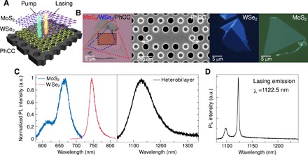
Fig. 1. MoS2/WSe2 heterobilayer-PhCC nanolaser.

(A) 3D schematic image of the fabricated heterobilayer-PhCC nanolaser. (B) First panel: Optical microscope image of MoS2/WSe2 heterobilayer on silicon PhCC. The MoS2 monolayers, WSe2 monolayers, and PhCC are indicated by the red, blue, and black dashed lines, respectively. Second panel: Top-view scanning electron micrograph around the defect region of the L3-type defect silicon PhCC. The arrows show the displacement of the two end-holes by 0.163a (48.4 nm). The radius of other gray holes is shrunk to be ~62.4 nm to enhance the far-field vertical coupling. Third and fourth panels: Optical microscope image of WSe2 and MoS2 monolayers on PDMS before transfer, respectively. (C) Interlayer excitonic emission in MoS2/WSe2 heterobilayer compared with the intralayer emission in the two constituents. The spectra of monolayers were measured at room temperature with an excitation of 532 nm, and the spectrum of heterobilayer was measured at 5 K with an excitation of 740 nm. a.u., arbitrary units. (D) Cavity lasing mode emission spectrum taken at a continuous-wave pump power of 190 μW (T = 5 K). Lasing action occurs at λ = 1122.5 nm with a measured linewidth of ~2.7 nm.
