
Figure 4.
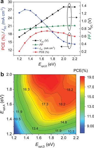
a) Evolution of the figures of merit of a single‐junction OPV device as a function of donor optical bandgap (E opt,D) with NFA optical bandgap (E opt,A) of 2.0 eV. This figure highlights the importance of maintaining balance between photocurrent gain and V OC reduction. b) Efficiency prediction (plotted in color scale, with numbers on the contour lines representing PCE in %) for NFA OPVs as a function of the donor and NFA bandgap (E opt,D and E opt,A). Input parameters: active layer thickness = 100 nm, and μh = μe = 5 × 10⁻⁴ cm2 V−1 s−1.