
FIGURE 1.
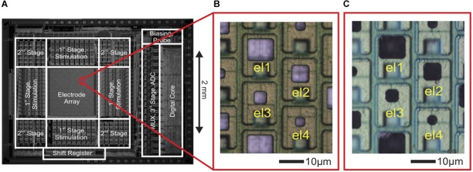
CMOS high-density microelectrode array (HD-MEA) and electrodes of varying size. (A) Die micrograph of the CMOS-based microelectrode system (Frey et al., 2009, 2010), fabricated in a 0.6-μm CMOS 3M2P process, that was used for extracellular neuronal recording and stimulation. The electrode array was integrated into a microsystem chip and featured a total of 11,011 electrodes in an area of 1.99 × 1.75 mm2. (B) Bright Pt electrodes of four different sizes (el1: 10 × 8.6 μm2, el2: 6.6 × 6.6 μm2, el3: 4.7 × 4.7 μm2, el4: 3.3 × 3.3 μm2). (C) The same electrodes after Pt-black deposition.