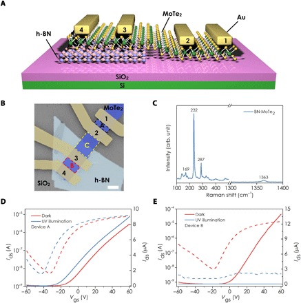
Fig. 1. Device architecture and electrical properties.

(A) Schematic of a junction device used in the study. The MoTe2 flake is a configurable semiconducting channel. The Si/SiO2 substrate serves as a back gate. Under the left half of the MoTe2 flake, we inserted a BN layer to create a BN/SiO2 interface. (B) False-colored SEM image of the device. The light blue and dark blue regions are the sections with and without the BN “cushion” layer. The black and red dashed rectangles mark the transport channels defined by two pairs of metal electrodes, named device A and device B, respectively. The junction region between electrodes 2 and 3 is highlighted by the yellow dashed rectangle and named device C. Scale bar, 5 μm. (C) Raman spectrum of a MoTe2/BN bilayer sample. Transfer characteristics of device A (D) and device B (E) in both linear (solid line) and semi-log (dashed line) scales. The Vds was 500 mV. Despite similar characteristics in a dark environment, the two devices demonstrated entirely different behaviors under UV illumination.
